
4H-SiC substrates for power semiconductors — Schottky diodes and MOSFETs. The SKUs divide the way a fab's demand does: by grade (prime for device runs, dummy and test for process setup) and by whether the wafer arrives bare or with an epitaxial layer already grown to your specification.
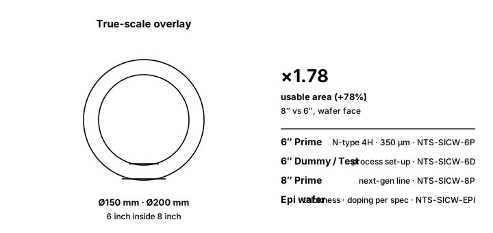
The 8-inch face carries about 1.78× the usable area of a 6-inch — the ~78% gain that pulls device lines toward the larger format.
Grades
| SKU | Grade | Typical | Application |
|---|---|---|---|
| NTS-SICW-6P | 6" Prime | N-type 4H, 350 µm class, micropipe density agreed per order | Device production and development |
| NTS-SICW-6D | 6" Dummy / Test | N-type 4H | Process setup and tool tests |
| NTS-SICW-8P | 8" Prime | N-type 4H | Next-generation lines |
| NTS-SICW-EPI | Epitaxial wafer | Thickness and doping to your specification | Single-sourced epi procurement |
NTS-SICW-6P — 6-inch prime
N-type 4H substrates in the 350 µm thickness class for device production and development runs. Micropipe density and the remaining defect criteria are agreed per order, because the level a diode run tolerates and the level a MOSFET run tolerates are not the same number.
NTS-SICW-6D — 6-inch dummy / test
The same format without the prime-grade defect criteria, for process setup, equipment qualification and short-loop tests — consumption that should not burn prime material.
NTS-SICW-8P — 8-inch prime
N-type 4H prime substrates in the 8-inch format for next-generation lines. Availability is specification-dependent; send the specification you intend to run and we reply on feasibility first.
NTS-SICW-EPI — Epitaxial wafers
Substrate and epi delivered as one purchase, thickness and doping to your specification. We review the epi specification sheet and cross-check it against each manufacturer's own format, because the same target is written differently from one epi house to another and the differences surface as yield, not as paperwork.